@Vengineerの戯言 : Twitter
SystemVerilogの世界へようこそ、すべては、SystemC v0.9公開から始まった
このブログでも何度も取り上げている Graphcore 。
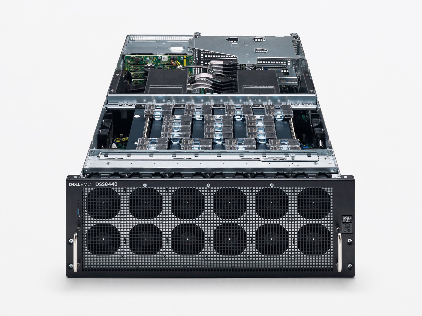
学習用チップで、PCIe ボード上に2個載ったものがDellのサーバーに8枚ささっているものが Microsoftのクラウドにて利用できるようになっています。
Dellのサーバー(4U)は、下のような写真(URLで引用します)がGraphcoreのサイトにあります。
そんな Graphcore ですが、このブログで取り上げたのは、なんと2017-04-30です。2年半も前です。
実際にチップが出てきたのが2018年11月。
この時点での情報は、
- チップ名:Colossus GC2
- IPU-Cores なるものが1216個搭載
- 各IPUは、100GFlopsでかつ、7スレッド
- チップあたり300MBのSRAM、30TB/sのメモリ帯域
- 各IPUは、low precision floating pointをサポート
- 23.6Bトランジスタ。。。
- 80 IPU-Links なるチップ間インターコネクトにて、2.5Tbpsの転送レート
- チップ間転送では、IPU-Exchangeなるもので、8TB/sの転送レート。
- PCIe Gen 4 x16
でした。
そして、最新情報は、GraphcoreのProducts/ipu にあります。その中の数をURLで引用し、表示します。この図には、
- IPU-Tiles TM (1216 IPU-Tiles each with an independent, IPU-Core and tightly coupled In-Processor-Memory)
- IPU-Core TM (1216 IPU-Core with 7296 programs executing in parallel)
- In-Processor Memory TM (300MB In-Processor-Memory, 45TB/s memory bandwidth, While model held on-chip)
- IPU-Exchange TM (8 TB/s all to all IPU-Exchange, Non-blocking, and communication pattern)
- IPU-Links TM (80 IPU-Links, 3200GB/s chip to chip bandwidth)
- PCIe Gen4 x16
のように、すべてに TM が付いています。
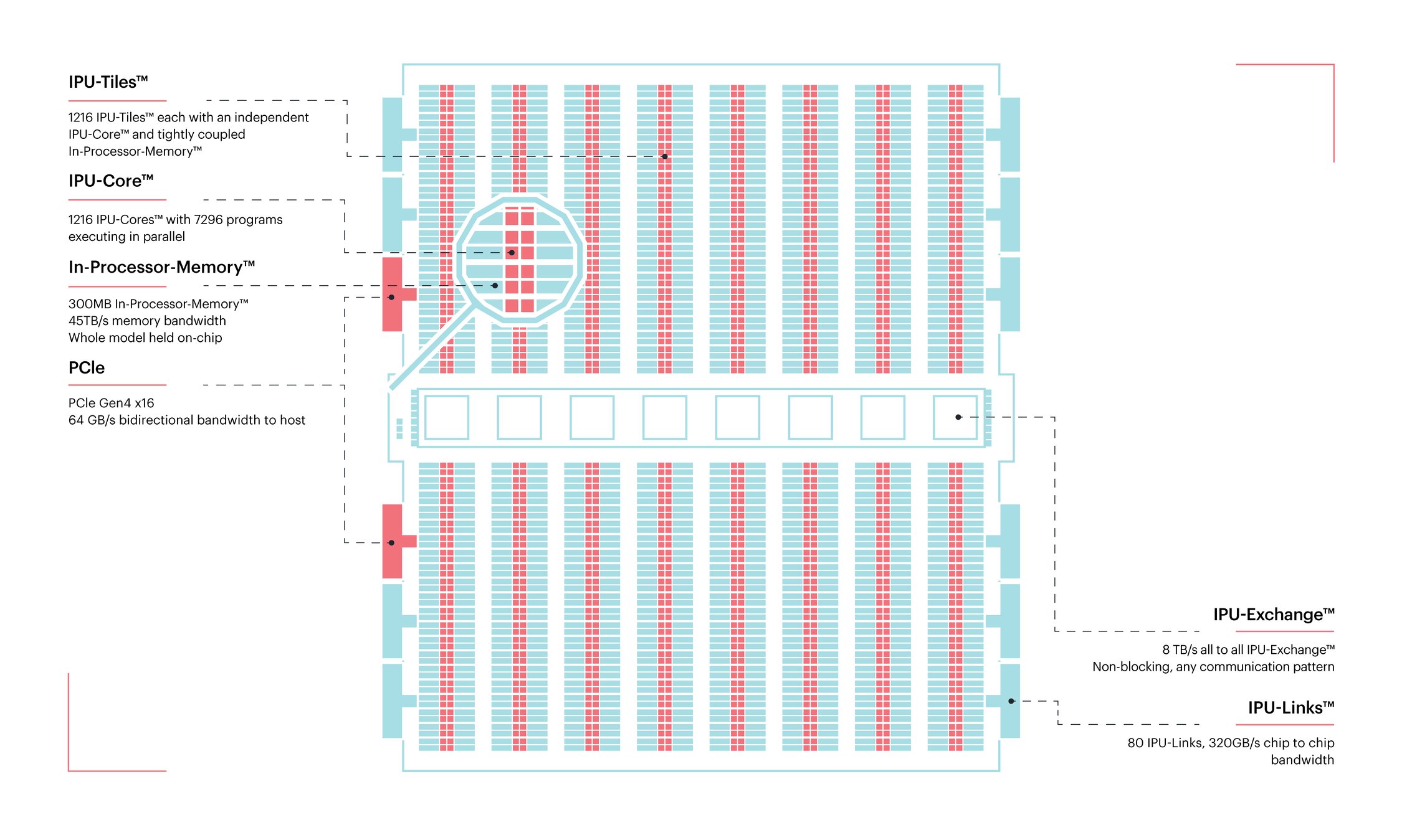
- 基本的には追加された情報は無いですね。
- IPU-LinkとPCIeは基本的には同じSerDes使っていそう
- IPU-Coreに対して、In-Processor-Memoryが約250KB
- Thread数は、7ではなく、6(7296 programs / 1216 IPU-Core)
- In-Processor-Memory の帯域が 30TB/s から 45TB/s にアップ
- IPU-Links の帯域が 2.5TB/s かあ 3.2TB/s にアップ
下記がこのブログで紹介した Graphcore 。