はじめに
先週、GoogleはTPU v4に関する論文、「TPU v4: An Optically Reconfigurable Supercomputer for Machine Learning with Hardware Support for Embeddings」を公開しました。
ちなみに、各バージョンのTPUは下記の時期の発表されています。
- TPU v2 の発表は、2017.5.17 (Google I/O 2017)
- TPU v3 の発表は、2018.5.8 (Google I/O 2018)
- TPU v4 の発表は、2021.5.18 (Google I/O 2021) (発表前の2020 年 7 月、2021 年 1 月 MLPerf トレーニング結果を提出している)
- TPU v4i : ISCA2021、2021.6.14
Hotchips の講演資料
- HotChips 2019 Tutorial, Cloud TPU: Codesigning Architecture and Infrastructure
- HotChips 2020, Google’s Training Chips Revealed: TPUv2 and TPUv3
- HotChips ML Tutorial 2021, Challenges in large scale training of Giant Transformers on Google TPU machines
このブログでは、Google TPU に関しては、下記の内容をアップしています。
- 2021-06-13 : Google TPU v2/v3/v4 の interconnect について
- 2021-06-28 : Google TPU v4i、Inference Onlyチップ
- 2023-01-26 : Google TPUのドキュメントが更新されていた
Google TPU v4 については、既にシステムアーキテクチャにてかなり公開されています。
今回の論文の中で、TensorCoreではなく、SparseCoreなるものの説明がありましたので、見ていきます。
SparseCore
以下、図および文章を、上記論文から説明のために引用します。
SparseCoreが何のためにあるのか?
Performance could be optimized using the total HBM capacity of a TPU supercomputer, joined by a dedicated ICI network, and with fast gather/scatter memory access support. This led to the codesign of the SparseCore (SC).
- with fast gather/scatter memory access support
The SC is a domain-specific architecture for embedding training starting with TPU v2, with later improvements in TPU v3 and TPU v4. SC is relatively inexpensive, at only ~5% of the die area and ~5% of the power. SCs operate in a sea-of-cores configuration, combining supercomputer-scale HBM and ICI to create a flat, globally addressable memory space (128 TiB in TPU v4). In contrast to all-reduces of large parameter tensors in dense training, the all-to-all transfers of smaller embedding vectors use HBM and ICI with finer-grained access patterns for scatter/gather.
- SparseCoreは、チップに4個は入っているようです。SparseCoreはv4で初めて導入されたものではなく、v2からあるようです。v3では2個載っています。
- TPU v4 のメモリ空間は、128TiB 。TPU v4 POD は、4096個のTPU。1個のTPUには32GBのHBMなので、32GB x 4096 = 128TB になります。
As separate cores, SCs allow parallelization across dense compute, SC, and ICI communications. Figure 7 shows the SC block diagram, which we consider a “dataflow” architecture because data flows from memory to a variety of directly connected specialized compute units.
下図(Figure 7)は、SparseCore のブロック図です。OCIというところと接続しているみたいです。

この論文では、TPU v4 の内部ブロック図は明記していませんが、TPU v4i の論文「Ten Lessons From Three Generations Shaped Google’s TPUv4i」に TPU v4iのブロック図が載っています。説明のために下記に引用します。
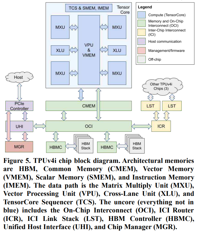
上図にあるように、OCI とは、On Chip Interconnect で、2個のHBM Controller、ICR (ICI Router)、UHI (Unified Host Interface)、CMEM (Common Memory)、TensorCoreと接続しています。
The most general SC units are the 16 compute tiles (dark blue boxes in Figure 7). Each tile has an associated HBM channel and supports multiple outstanding memory accesses.
SparseCore には、16個のcompute tilesがあって、各 tile は HBM のチャネル (16チャネル)に対応していて、16個同時にメモリアクセスできるようになっていると。。。
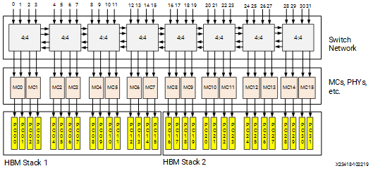
となると、HBM Controller は 16ポートになってる可能性が高いですね。。。
下図は、Xilinx社のHBM Controller IPに関する図です。ここから説明のために引用します。HBMに対して16ポートあるのがわかります。こんな感じに OCI から HBMC に繋がっているんでしょうかね。
Each tile has a Fetch Unit, a programmable 8-wide SIMD Vector Processing Unit (scVPU, not to be confused with VPU of the TC in TPU v4), and a Flush Unit. The Fetch Unit reads activations and parameters from the HBM into the tile’s slice of a 2.5 MiB Sparse Vector Memory (Spmem). The scVPU uses the same ALUs as TC's VPU. The Flush Unit writes updated parameters to HBM during the backward pass.
各Tileには Spmem (SparseCore当たり、2.5MB)が付いていて、ALUはTensorCore内のVPUと同じものを使っている。backward pass時に、Flush Unitが更新したパラメータをHBMに書き戻す
In addition, the five Cross-Channel Units (gold boxes in Figure 7) perform specific embedding operations, which their names explain. Like TPU v1, the units execute CISC-like instructions and operate on variable-length inputs, where the run-time of each instruction is data-dependent. The cross-channel units operate across all 16 banks of Spmem collectively.
おわりに
Google TPU には、TensorCoreだけでなく、SparseCoreなるものが入っているんですね。。。これ、大規模なシステムには必要なんですかね。
関連記事