@Vengineerの戯言 : Twitter SystemVerilogの世界へようこそ、すべては、SystemC v0.9公開から始まった
はじめに
Googleが 2021 ACM/IEEE 48th Annual International Symposium on Computer Architecture (ISCA) にて、
Ten Lessons From Three Generations Shaped Google’s TPUv4i
なるタイトルで講演したようです。TPU v4 ではなく、TPU v4i です。
論文は、ここ にありました。
TPU v4i の特徴
- 7nm (v2/v3 : 16nm)
- Perf/CapEx ではなく、Perf/TCO が重要
- v2/v3 と Compiler compatibility, not binay compatibility (推論だけど、bf16, fp32をサポート)、int8もサポート
- v2に対して、v3と同じぐらいの性能向上があるが、消費電力費ではv3 に比べて2.3倍以上いい。
- v4iの命令は、v3の命令 より25%ワイド
- 4 MXU/1コア
- SRAM 144MB (Vector Memory : 16MB + Common Memory : 128MB <= 新規)
- TensorCore DMA は、v2/v3の two-dimensional (single-strided) から four-dimensional (triple-strided)
- TPUv4i unifies the DMA architecture across local (on-chip), remote (chip-to-chip), and host (host-to-chip and chip-to-host) transfers to simplify scaling of applications from a single chip to a complete system.
- 内部でデータ幅は、512B
- 1.0GHz で動いて、TDP が 175W
- HBM2 8GB (4GB x 2)
- tracing and performance counter の追加
- 1コア/1チップ (チップサイズは、v1 = 330 mm2, v2 = 625 mm2, v3 = 700 mm2, v4i = 400mm2)
- 4チップ/1ボード (4チップはリングで接続)
- 2ボード/1ホスト
- 空冷
MXU は、128x128 なので、x4だと、256 x 256 になり、TPU v1 と同じ感じになりますね。
下記に説明のために、Figure 7. を引用します。
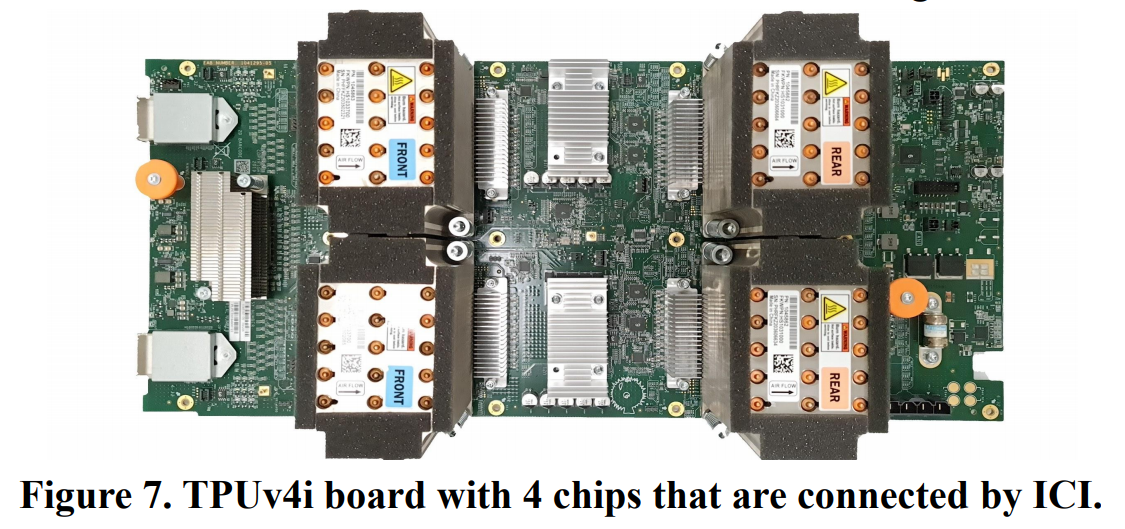
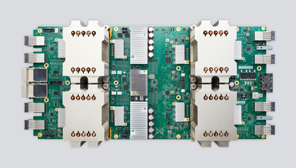
Google TPU v2 の写真と比較すると、かなり似ています。(比較のために、ここ から引用します)
チップ間のインターコネクトは、4本から2本になっています。このため、ボード外への接続が無くなっています。
タイトルにある、10個のレッスンとは?
- Logic, wires, SRAM, & DRAM improve unequally
- Leverage prior compiler optimizations
- Design for performance per TCO vs per CapEx
- Support Backwards ML Compatibility
- Inference DSAs need air cooling for global scale
- Some inference apps need floating point arithmetic
- Production inference normally needs multi-tenancy
- DNNs grow ~1.5x/year in memory and compute
- DNN workloads evolve with DNN breakthroughs
- Inference SLO limit is P99 latency, not batch size
この論文では、この10個のレッスンについて、語られています。
おわりに
今回の TPU v4i を知ったのは、Tensor Processing Unit の Wikipedia です。ここに、TPU v4 なるものの詳細が載っていました。その出典が今回の論文、こちら, スライド もだったわけです。Wikipedia では TPUv4 とありますが、TPU v4i です。Inference Onlyということでした。
論文の最後に、
With Moore's Law diminishing and Dennard scaling dead, hardware/software/DNN co-design is the best chance for DNN DSAs to keep vaulting accelerator walls.
とありました。そうなんだ。
P.S 論文の中に、
Google deployed the single core TPUv4i for inference and the dual core TPUv4, which scales to 4096 chips, for training. Google previewed TPU v4 as part of the MLPerf Training 0.7 in July 2020, where it was 2.7X faster than TPUv3.
とありました。となるということは、TPU v4 は v4i の2倍って感じなんですかね。。。たぶん、HBM2メモリの容量は2倍の16GBということはないでしょうが。